I have been developing further the methodology of DIY-CAD (formerly known as “children aided design”). And did a series of workshops over the course of the last couple of months. Amazing and diverse outputs, always nice to see what creative people without background in engineering or circuit design come up with.

Creative output of the “Draw your own PCB” workshop in Gudskul, Jakarta.
I have been introducing this method already back in 2017 in Chile, mbe some of you remember.
I am convinced, that as a very playful and almost zero-cost workshop, many fundamental concepts of open science hardware can be introduced by this method. And it’s open-ended to more “expert” introductions before going on towards a software workshop, such as kicad.
The workshop concept can easily be shared globally, all it needs is to print out the handouts, get some pens, pencils, erasers, paper and a kinda transparent cover to finalize the copper design. All that stuff should be available in a common stationary store worldwide.
Some of the fundamental topics and learnings are:
- Open Hardware is about redesigning existing shared knowledge to your own needs / creativity
- A shared schematics shows the abstract “function” of an electronic device
- The selection of the BOM (bill of materials) will decide on exactly which parts are used, according to your wishes or availability of them in your local environment
- Parts placement on paper to come up with your own layout / interface design
- Implement the connectivity (kinda ratsnest), from schema to functional hardware
- Draw the copper layer creatively
- Add logos, credits and decorational designs
- Share your designs to bring them back into the pool of design and knowledge of open hardware
The designs can then be scanned or photographed, re-scaled into the “real” size, and either used for DIY etching into copper boards, or prepared for manufacturing using open source software and inkscape extensions svg2shenzhen together with kicad, to get the gerber files.

Some impressions of the GAPS workshop during Electric Wonderland in Croatia
If more time is available with inkscape and svg2shenzhen, all the other “layers” for manufacturing can be introduced:
- solder mask and silkscreen
- double sided boards
- drill holes
- edge cut
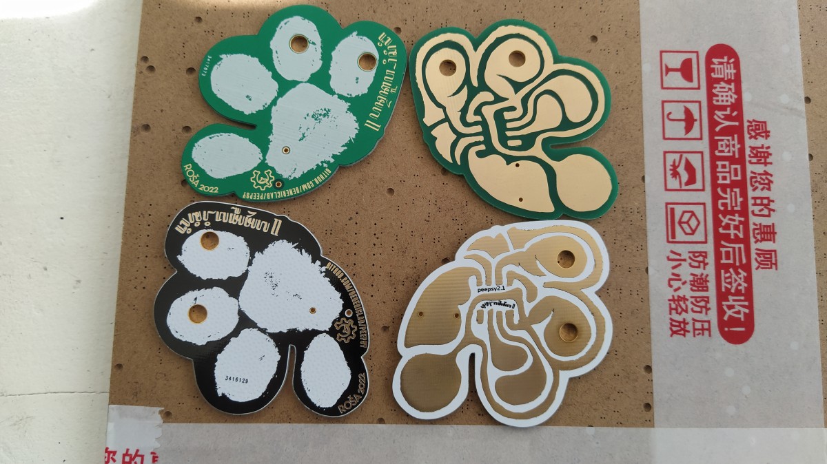
Manufactured boards from the output of the GAPS-peepsy worshop in Yogyakarta
I made 2 new versions of doing such a workshop:
Peepsy - simple continuity tester
Very simple schematic and easy to layout. The product is even something useful for everybody who likes hardware and electronics. It’s a “continuity” tester, that one function on every multimeter, that we use the most!
It uses almost now power, as the attiny85 microcontroller goes to sleep all the time.
See info on github: GitHub - GenericLab/peepsy: simple continuity tester
Based on Continuity Tester by David Johnson-Davies - www.technoblogy.co
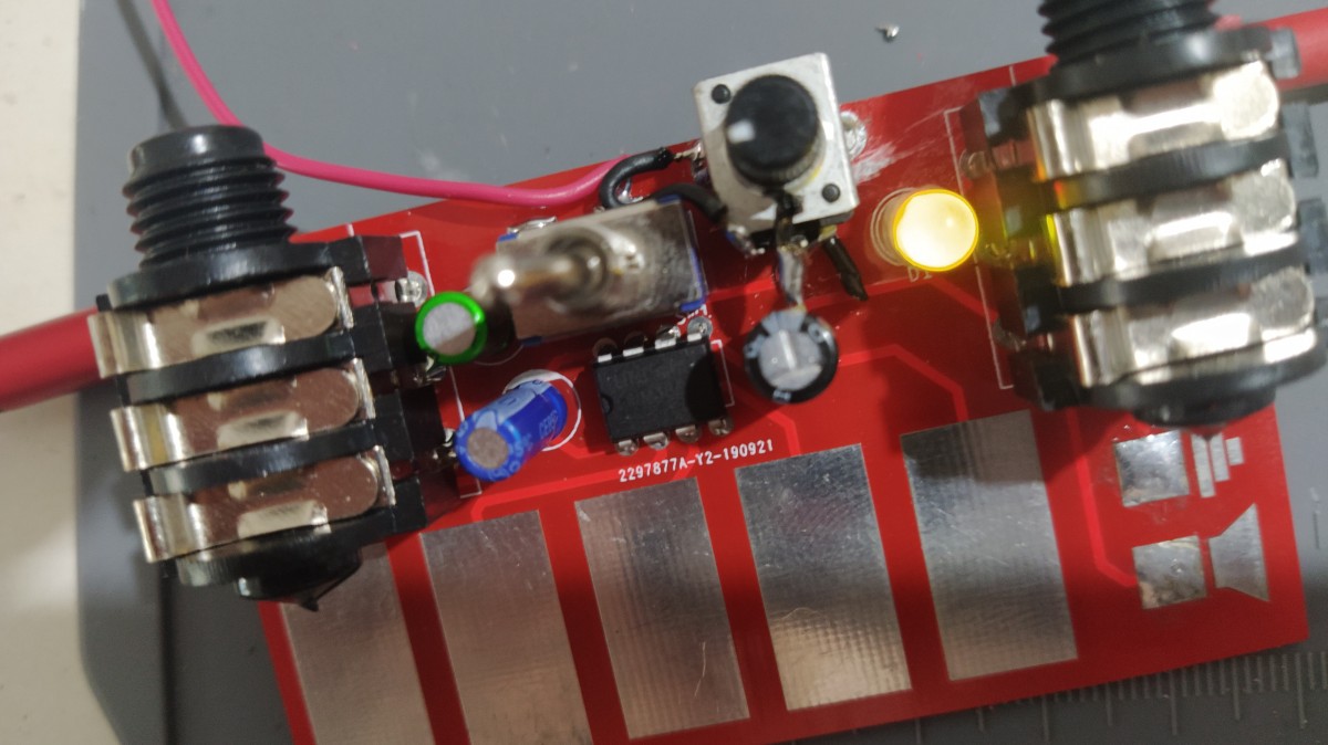
DangdutFromHell - Touch Noise Syntesizer
For the more sound related and noise geeks, i just developed another module using the most common audio amplification chip, LM386. The circuit has an input and an output, can be used as an amp to drive a speaker, and the gain is so high, that with the potentiometer we can go far into distortion of the input. Additional touch-pads can be used to “f# up” the sound completely and bend / hack the chip to make it scream and make many weird noises.
See info on github: https://github.com/dusjagr/GAPS-DangdutFromHell
Example of a design for this circuit, by Alwin Weber from CircuitControl