[Day 3] KiCAD PCB Designing Workshop

Hi Guys,

Here you go. Thanks to @kaspar for facilitating the session.

Paricipants:
1. Isaac
2. Tamara
3. Pollock
4. Carmen
5. Tony Yet
6. Akshai M

Steps Involved :

  1. Make a new project.

  2. Think of a circuit, LED Circuit.

  3. Select Eeschema.

  4. Place components. Use shortcuts “A” to do placing. “R” to rotate. “M” to move.

  5. Place wires.
    kicad_1

  6. Mark the values using “E”
    kicad_2

7.Annotate and do CvPCB to do footprint assignment. Generate Netlist

  1. Open PCB editor and load netlist route components.
  2. To use 3d viewer use Alt + 3.
  3. Add GOSH 2018 Badge !
  4. File >> Plot >> Gerbers. Share the gerbers to PCB Manufacturer.
  5. Use tracespace.io to view the PCB files.
2 Likes

Thanks Akshai, you even added pictures! If anyone has any questions about KiCad feel free to ask here. There is also a very active forum about KiCad:

Summary:

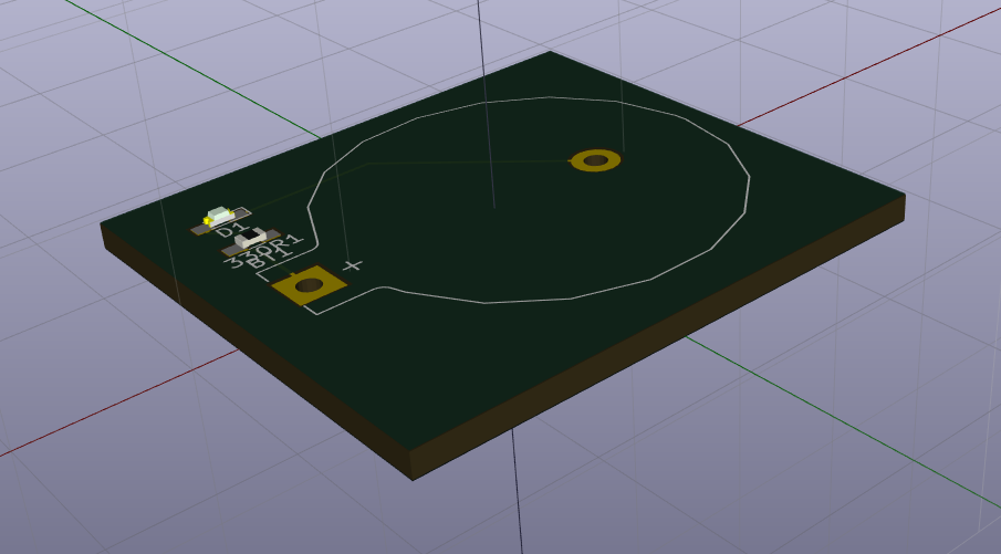
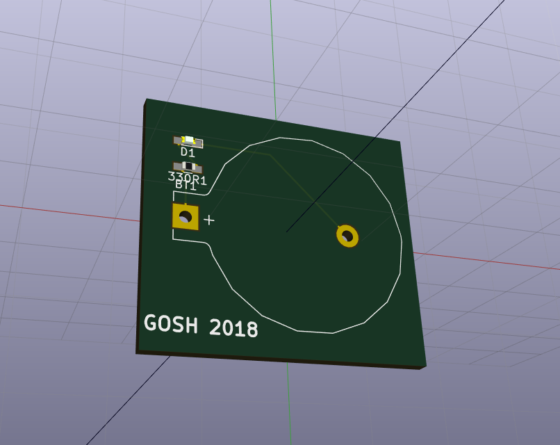
KiCad is the most popular and feature-rich free and open source electronics design automation (EDA) suite for printed circuit board (PCB) design in the world. EDA PCB software is used to design circuits and lay them out on a model of a physical board resulting in design files that allow PCBs to be manufactured. KiCad runs on Linux, Mac OS and Windows and receives development effort from a large group of volunteers as well as a handful of paid developers working for CERN.

Using free and open source software for open source hardware designs is important as it helps ensure people can make use of, study and re-purpose your designs without encountering restrictions such as licensing costs or fear of copyright infringement.